Author: |
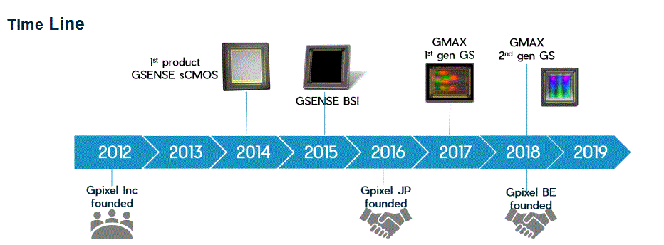
Founded in 2012 by experienced CMOS image sensor designers and semiconductor physicists, Gpixel works in close cooperation with our customers and business partners to produce state-of-art CMOS image sensors for use all over the world.
From our offices in Changchun, China (headquarters), Antwerp, Belgium (European design center) and Tokyo, Japan (Japanese design center) we are committed to delivering innovative and specialized high-end CMOS image sensor solutions for industrial, professional, medical, and scientific applications.
Global Shutter Pixels
No single application prefers RS pixel over GS pixel from shutter point of view. Gpixel has a portfolio of proven, state-of-the-art charge domain GS pixels
1. The world’s smallest GS pixel: down to 2.5 μm square pixel
2. High QE: > 65%
3. Very good Shutter Efficiency: < - 100 dB
4. Large Dynamic Range: 60-80 dB
5. 65 nm CIS technology with double in-pixel light pipes

Large Area CIS Design
Design for yield
1. Circuit layout avoiding device failures coming from wafer processing defects
2. Balance between performance and yield
1D/2D stitching
1. Know-how to design chips larger then photo lithography mask size (typ. ~ 32 x 25 mm)
2. Know-how to minimize image artefacts due to stitching
3. Support of 8” and 12” mm wafers by wafer foundry
4. Single mask set can be used to make different products (resolution variants)

GMAX1205
More products please click:
http://www.gpixelinc.com/en/index.php?s=/a/5.html

 中文
中文