浏览量:
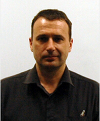
Speaker :Prof. Saulius Juodkazis
Time :June 21 ,2016 14:00
Location:The forth meeting room in Research Building
Hosted by: Division of International Cooperation
Report content: Future light-based technologies should deliver us energy, food, fast communications, and sensors in various fields of life. Light-matter interactions occurring on atomic and molecular level still need to be better understood and controlled for practical applications. We need tools which can control light at nanoscale and could be used for nano-fabrication and manipulation of nano-objects. In this talk our recent advances in high precision nanofabrication using 3D approaches and combining standard cleanroom tools with laser direct writing capabilities will be presented for optical sensors and high efficiency diffractive optical elements. Combination of electron beam lithography (EBL) with post-processing of nanoparticles with Ga-ion milling opens a possibility of sub-20 nm direct write of nano-inscriptions on nanoparticles. Arrays of identical nanoparticles were fabricated with high fidelity and with uniform nano-features. This approach was a key to make chiral plasmonic nanoparticles which show strong optical dichroism and can be used for optically driven motors and nano-tweezers. Surface charging which is a common problem in applications of ion milling and electron imaging is resolved with co-illumination of deep UV light whose photons have energy larger than the electron work function for a given material. Post-processing of single nanoparticles as well as THz antennas was made with focused ion beam lithography (IBL). EBL and IBL can be both optimized for a high throughput for simple sample geometries. 3D laser fabrication of micro-optical elements and nano-textured surfaces adds new applications in lab-on-chip and sensing. The talk will address current challenges in mechanical handling and fabrication for future instrumentation and characterisation in photonics.
Speaker CV: S.Juodkazis (PhD 1997 from Vilnius Univ., Lithuania and Lyon-I Univ., France) is currently investigating peculiarities of light-matter interaction in small space and time domains (sub-wavelength and sub-1 ps) for light harvesting, control and sensing applications. He setup a nanotechnology cleanroom facility in 2012 in Swinburne which hosts 10 nm resolution electron and ion lithography, plasma deposition and etching tools with an ultra-short laser processing setup all capable of 3D nano-micro-structuring of materials. He is a Fellow of OSA and SPIE, chair professor at Bordeaux University in France and Changjiang scholar at Jilin University, China. S. Juodkazis serves on editorial boards of several journals including Optics Express, also works for conference organizing and program committees

Prof. Saulius Juodkazis


 中文
中文

