Author: |
In the study published in the journal Light: Science & Applications, LI Dabing’s group from Changchun Institute of Optics, Fine Mechanics and Physics, Chinese Academy of Sciences (CAS) cooperating with Deng Huixiong from Institute of Semiconductors, CAS, have reported a method to realize high efficiency p-type in ultra-wide-gap III-nitrides by non-equilibrium quantum doping scheme.
AlGaN materials have direct and adjustable band-gaps, which are ideal materials for fabricating UVC light source. But the poor p-doping efficiency of high Al component AlGaN is one of the obstacles to hinder the performance. It originates from the high activation energy due to the deep acceptor level. This physical limitation is widely observed in wide-gap semiconductors.
The development of new doping methods to reduce the activation energy of acceptor is fundamental to improving the p-type doping efficiency of high Al content AlGaN materials and promoting the efficiency of deep UV light sources.
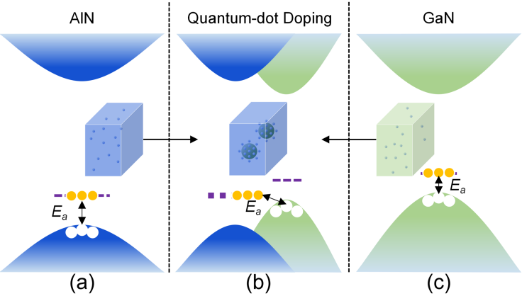
To this end, the researchers developed a quantum non-equilibrium doping method. By introducing GaN quantum structures next to the Mg-dopants into AlGaN matrix, the VBM of the system moved up. Consequently, the holes could effectively release to VBM with a much smaller activation energy than that for intrinsic system. First, a quantum engineering doping model was constructed by systemically first-principles calculation. It was found that the introduction of GaN quantum dots into AlN materials can effectively raise the VBM of the system. Second, the AlGaN:GaN quantum dots were grown by developing the "discontinuous epitaxy" scheme based on metal organic chemical vapor deposition (MOCVD).
The activation energies of Mg acceptors were smaller than 50 meV, which was about an order of magnitude lower than that for intrinsic materials. The hole concentrations were up to 1018 cm-3, which reaching the international advanced level. The performance of the deep UV LED based on the non-equilibrium quantum doping method was significantly improved.
This work improves the efficiency of optoelectronic devices based on ultra-wide-gap nitrides and provides a new solution to the doping problem of other ultra-wide-gap materials, which is expected to promote the development of the ultra-wide-gap semiconductor industry.

FIG. VB modulation mode to lower the acceptor Ea in UWBG Nitrides. Acceptors are randomly doped in (a) AlN and (c) GaN. Both have high Ea in this condition. (b) GaN-QDs are embedded in AlN matrix and acceptors are doped in AlN matrix and concentrate near the interface. (Photo by CIOMP)
Contact
Auther: SHI Zhiming
Changchun Institute of Optics, Fine Mechanics and Physics, Chinese Academy of Sciences
Changchun, Jilin 130033, China
E-mail: shizm@ciomp.ac.cn
Article links: https://www.nature.com/articles/s41377-021-00503-y
