Author: |
Editor: Amer Kotb | Oct 15, 2021
In the future, all-optical signal processing is likely to play a bigger role in ultrahigh-capacity communications networks. All-optical logic technology development is critical for a variety of applications in all-optical networks, including high-speed all-optical packet routing and optical encryption. A demonstration of optical logic elements and circuits that can work at high speeds is an essential step in the development of this technology. These logic elements include the traditional Boolean logic functions such as NOT, AND, OR, XOR, NAND, NOR, and XNOR, and circuits such as parity checker, all-optical adder, and shift register.
On the other hand, metasurfaces have recently attracted strong interests in nanophotonic device development owing to their unique features including compactness, low loss, and low-temperature dependence. A metasurface is an artificial nanostructured interface with subwavelength ultrathin film. Dielectric-loaded waveguides are also used in the design and fabrication of many passive photonic devices.
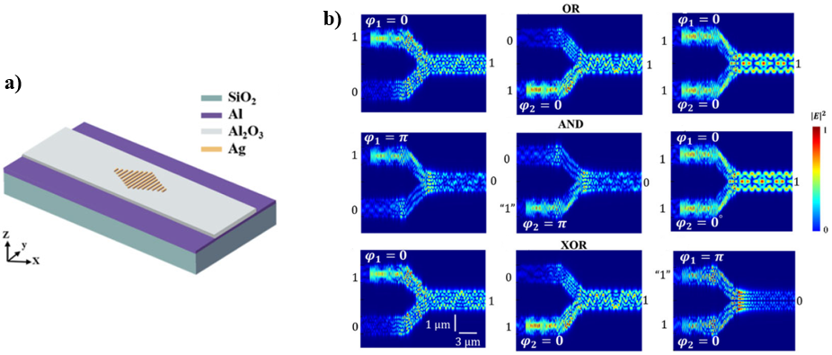
Scientists at the Changchun Institute of Optics, Fine Mechanics, and Physics of the Chinese Academy of Sciences have collaborated with scientists from the University of Rochester to simulate a novel metasurface having quasi-rhombus-shaped antennas to modulate optical modes in a dielectric-loaded waveguide for the realization of a complete family of all-optical logic operations, including NOT, AND, OR, XOR, NAND, NOR, and XNOR.
Scientists in China and America designed a quasi-rhombus metasurface with a silver (Ag) nanorods antennas patterned directly at the top surface of the dielectric-loaded waveguides. Owing to the high transparency and high sensitivity of Al and Al2O3 in the UV-visible spectra region along with their CMOS compatibility, and ease of integration with the mature Si microelectronics, the dielectric-loaded waveguides is designed with 200 nm thick Al2O3 ridge on the surface of 100 nm thin Al on a glass substrate. Scientists took advantage of this unique design to realize all-optical NOT, AND, OR, XOR, NAND, NOR, and XNOR logic operations with a speed as high as 108 Gb/s. The operational principles of these gates are based on the constructive and destructive interferences caused by the difference in the phase of the input signals.
In performance comparison with the previously reported waveguides, high contrast ratios have been achieved for the considered Boolean functions using the proposed structure. These important results for optical communications applications have been published immediately after being submitted to a journal of Optics Letters (https://doi.org/10.1364/OL.396978).

a) Schematic illustration of quasi-rhombus metasurface with dielectric-loaded waveguide and b) distribution of field intensity for OR gates, AND gates, and XOR logic gates.(Image by Kotb)
