Author: |
Editor: Amer Kotb | Oct 19, 2021
The core parts for optical data processing are all-optical logic gates, which are projected to play a critical role in future ultrafast high-capacity communications networks. However, while these logic functions are handled by highly limited and high-cost single-function logic operations, the necessity for high capacity and low-cost signal processing became imperative.
Professor Chunlei Guo at the University of Rochester and his co-author Dr. Amer Kotb at the Changchun Institute of Optics, Fine Mechanics, and Physics of the Chinese Academy of Sciences have collaborated to overcome the single-function limitation by investigating through means of theoretical analysis the performance of all-optical multifunctional six basic logic gates, AND, NOR, XOR, OR, XNOR, and NAND, for the first time using the nonlinearity properties of cross-phase modulation in a single compact scheme based on few semiconductor optical amplifiers (SOAs) at a data rate of 100 Gb/s. The AND and XOR logic gates are implemented using SOA-assisted Mach-Zehnder interferometers in this study, whereas the NOR logic gate is implemented utilizing a single SOA and a delayed interferometer. The outputs of the AND, XOR, and NOR logic gates are then combined to generate three further logic gates: OR, XNOR, and NAND. Three measures, namely quality factor, extinction ratio, and contrast ratio, are used to assess the performance of the Boolean functions under consideration.
Simultaneously, it is desirable to conduct six logic functions without having to modify the switching module or the way it is configured or driven each time, in order to enable smart, adaptable, dependable, and repeatable operations. As a result, this compact system saves time, money, and complexity. High-performance integrated photonic circuits can also be built using this scheme.
The Wolfram Mathematica results show that the proposed compact approach at 100 Gb/s can be used to study six basic logic functions with higher performance. It is worth noting that 100 Gb/s optical links are widely used today in data centers.
This paper won the admiration of the scientific community accused of this field, as it reaped many citations as soon as it appeared in Optics and Laser Technology (https://doi.org/10.1016/j.optlastec.2020.106828). After many years of research, our scientists were able to design six logic gates using a very small scheme that operates at a high speed.
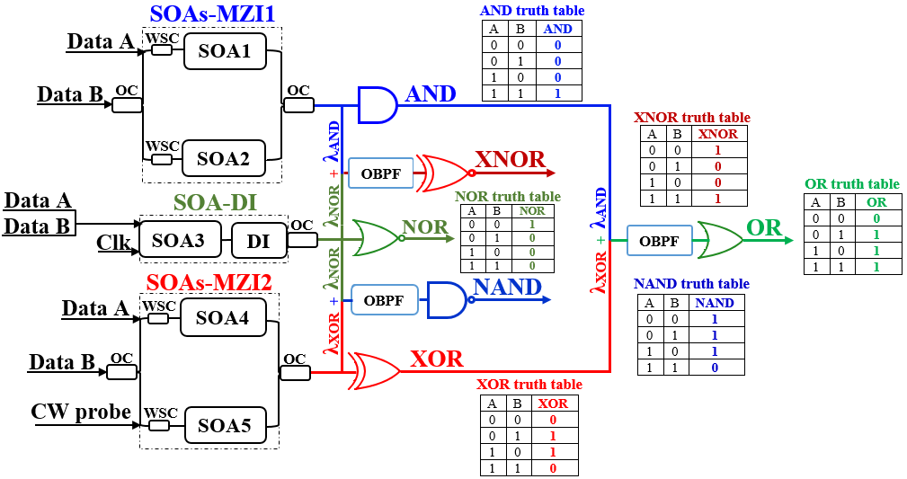
All-optical multifunctional AND, NOR, XOR, OR, XNOR, and NAND logic gates in a single compact scheme based on SOAs.

 中文
中文