Author: CHEN Tianbao |
The Segmented Planar Imaging Detector for Electro-optical Reconnaissance (SPIDER) imager has attracted intensive attention because of its superior imaging performance and structural compactness. This new imaging method has been proposed based on standard imaging interferometer techniques. Through introducing photonic integrated circuits (PICs) and replacing bulk lens systems with compact lenslets array, the SPIDER is estimated to reduce size, weight, and power (SWaP) by about ten to hundred times for a similar resolution compared with conventional diffraction-limited optical systems.
Several lens array patterns have been proposed to acquire higher imaging quality, These patterns providing low-frequency intensive but high-frequency sparse measurements of the visibility function. In a study published on Optics Communications, a research group led by Prof. ZHANG Xuejun from Changchun Institute of Optics, Fine Mechanics and Physics (CIOMP) of the Chinese Academy of Sciences (CAS) indicated that sparse measurements of high-frequency visibility introduce Gibbs-ringing artifacts in the image reconstruction, severely damaging the imaging quality of SPIDER.
Therefore, Prof. ZHANG Xuejun’s research group proposed a new simplified sparse-aperture photonics-integrated interferometer (SPIN) imaging system on Optics Express. The SPIN yields enhanced optical transfer function, which makes Gibbs-ringing artifacts less obvious. Hence, the imaging quality with equivalent aperture diameter is improved. Further, the SPIN imaging system was designed as a Fizeau configuration interferometer imaging system, which is different from Michelson configuration interferometer as SPIDER. This transfer of configuration type provides a more concise structure. As a result, the SPIN can be designed with fewer wavebands and fewer apertures.
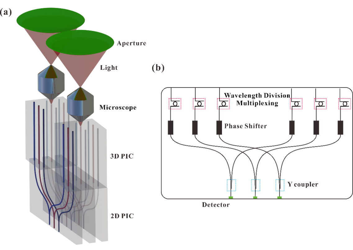
A conceptual diagram of SPIN with two apertures is depicted, including waveguide path layout and functional structure schematic of Photonic Integrated Chip (PIC). The microscope is used to eliminate the apodization effect, which is caused by the coupling effect between lenslet and waveguide. The waveguide array is adopted to receive fine details and enlarge the field of view (FOV). The density of waveguide is determined by aperture configuration and microscope. In addition, the crosstalk between waveguides is inevitable, therefore, special designing of the length of waveguide array is analyzed according to the coupled-mode theory.
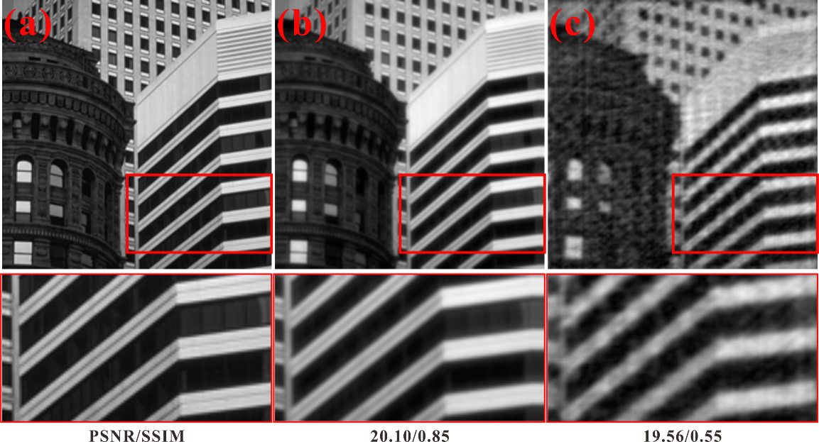
Based on analyses of apodization effect, FOV and crosstalks, the imaging principle was derived and revealed that the received image is degraded by point speas dunction and noise. Therefore, a hyper-Laplacian-based imaging reconstruction algorithm was developed. A simulation of the SPIN imaging system with seven apertures and one imaging waveband was demonstrated, and the imaging qualities of SPIN and SPIDER were compared with the same aperture diameter. It was demonstrated that SPIN has higher quality imaging performance.

(a) Conceptual diagram of optical waveguide path layout using 3D PIC and 2D PIC with two apertures in SPIN and (b) functional structure schematic of 2D PIC (Image by CHEN).

Illustration of the degraded images with different systems. (a) Original clear image. (b) Degraded image of SPIN imaging system. (c) Degraded image of SPIDER imaging system with direct IFT (Image by CHEN).
ZHANG Xuejun
Changchun Institute of Optics, Fine Mechanics and Physics
E-mail: zxj@ciomp.ac.cn
